

Working principle of semiconductor diode
Working principle of semiconductor diode
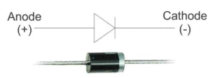
We know that a diode is a two terminal semiconductor device that conducts current primarily in one direction.
Study smarter with VoltageLab
Built for electricians, apprentices, and electrical engineers who want faster practice and better exam prep.
⭐️ Join thousands of electricians upgrading their skills
A diode has low resistance in one side where current can pass easily and high resistance in the other where current can’t pass. A diode can act as a switch.
A P-N junction is the simplest form of the semiconductor diode which behaves as an ideal short circuit in forward biased condition but opens in the reverse biased condition. The diode can convert AC to DC so sometimes it also called as a rectifier.
From the following picture, we can say that we can create a simple PN junction diode by doping donor impurity in one portion and acceptor impurity in other portion of silicon or germanium crystal block.
These doping make a PN junction at the middle part of the block beside which one portion becomes p-type and another portion becomes n-type.
We can likewise frame a PN intersection by joining a p-type (intrinsic semiconductor doped with a trivalent polluting influence) and the n-type semiconductor (characteristic semiconductor doped with a pentavalent contamination) together with an exceptional creation procedure.
Hence, it is a device with two components, the p-type shapes anode, and the n-type frames the cathode. These terminals are conveyed out to make the external connection.
Working principle of semiconductor diode
N-type have a significant number of free electrons and very few holes. But in P-type, It has a high concentration of holes and very few free electrons. For this reason, the free electron from n side will diffuse into the p side and recombine with holes present there, leaving position is not movable ions in n side and creating negative immobile ions in the p-type side of the diode.
Hence, revealed positive giver particles present in the n-type side close to the junction edge. Correspondingly, revealed negative acceptor particles present in the p-type side close to the junction edge.
For this reason, the number of positive ions and negative ions will accumulate on n-side and p side too. This region is formed the depletion region due to the free carrier in the region.
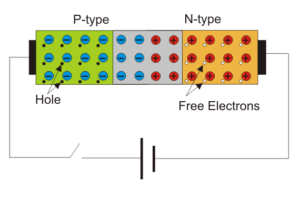
Because of the nearness of these positive and negative ions, a static electric field called as barrier potential is made over the PN junction of the diode. It is classified “barrier potential” since it goes about as an obstruction and opposes the further migration of gaps and free electrons over the junction.
