

Definition:
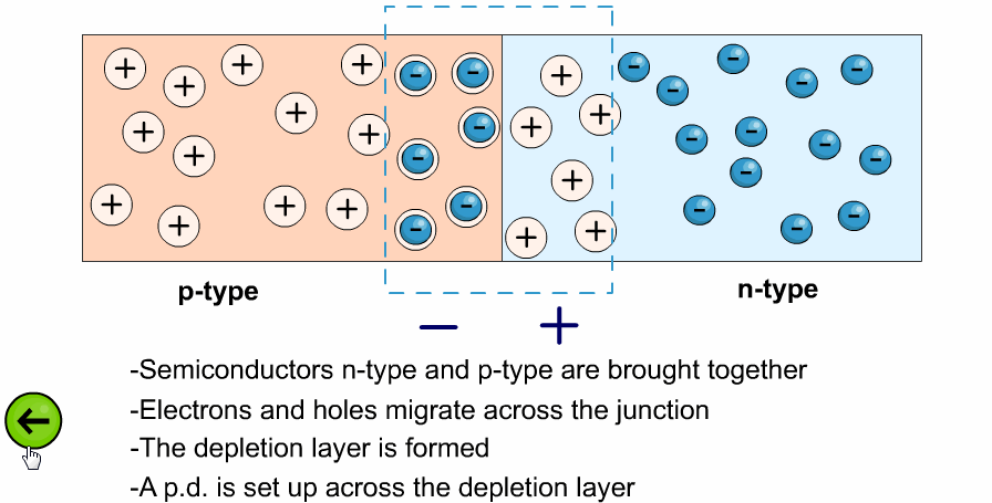
A PN junction diode is formed when a p-type semiconductor (rich in holes) is joined with an n-type semiconductor (rich in electrons). The junction between them allows current to flow in only one direction — making it the simplest and most widely used semiconductor device.
⚡ AI-Powered Electrician App
Study smarter with VoltageLab
Built for electricians, apprentices, and electrical engineers who want faster practice and better exam prep.
⭐️ Join thousands of electricians upgrading their skills
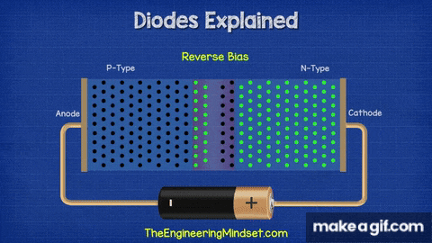
Explanation with GIF:
- The left side is the P-type region (black dots = holes).
- The right side is the N-type region (green dots = electrons).
- When connected as shown, the diode is in reverse bias — the positive terminal is connected to the N-side and the negative terminal to the P-side.
- This causes the depletion region at the junction to widen, blocking the flow of charge carriers.
- As a result, almost no current flows (except a tiny leakage current).
If the battery were reversed (forward bias):
- Electrons from the N-side and holes from the P-side would move towards the junction.
- The depletion region would shrink, and current would flow freely across the junction.
Quick Recap for Users:
- PN Junction = P-type + N-type semiconductor.
- Forward Bias: Current flows (depletion region shrinks).
- Reverse Bias: Current is blocked (depletion region widens).
- Main Use: Acts as a one-way switch for current — the basis of all diodes.